
The Z50Bus is a suggestion for a system expansion bus for 8-bit microcomputers. It’s designed to be compact, yet compatible, taking inspiration from previous standard bus layouts, and bringing it into a modern age. Being also inspired by the popular RC2014, it allows for easy adaptation of existing designs. The name of the Z50Bus comes from being originally designed to use a 50-pin connector to integrate a system around a Z80 CPU. Being a simple bus specification, it is possible to use/integrate it with other 8-bit CPUs using some glue logic.
Signal levels and descriptions
Signal levels are 5V Single Ended, with HC TTL levels expected. So, each signal uses a single line, and an active high signal will have a High at 3.5V – 5V, and a Low state at 0-1V. The 5V and GND lines are the only supply voltages on the bus. System implementations should make sure these are noise-free, well decoupled, and dimensioned for the system current draw.
The bus uses a double-row connector scheme, with the following pin layout
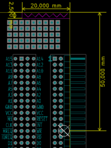
| Pin | Signal name | Pin | |
| 1 | A15 | A14 | 2 |
| 3 | A13 | A12 | 4 |
| 5 | A11 | A10 | 6 |
| 7 | A9 | A8 | 8 |
| 9 | A7 | A6 | 10 |
| 11 | A5 | A4 | 12 |
| 13 | A3 | A2 | 14 |
| 15 | A1 | A0 | 16 |
| 17 | Gnd | Gnd | 18 |
| 19 | 5V | 5V | 20 |
| 21 | /M1 | /Rst | 22 |
| 23 | Clock | /Int | 24 |
| 25 | /Mreq | /WR | 26 |
| 27 | /IOreq | /RD | 28 |
| 29 | D1 | D0 | 30 |
| 31 | D3 | D2 | 32 |
| 33 | D5 | D4 | 34 |
| 35 | D7 | D6 | 36 |
| 37 | Tx | Rx | 38 |
| 39 | Usr1 | Usr0 | 40 |
| 41 | Usr3 | Usr2 | 42 |
| 43 | /NMI | /Refresh | 44 |
| 45 | /Wait | /Halt | 46 |
| 47 | /BusRQ | /BusACK | 48 |
| 49 | IEO (*) | IEI (*) | 50 |
Female bus – Male card
* Note that IEO/IEI forms an Interrupt Enable Chain, where the IEO of a higher priority card needs to connect to a lower priority card. This means a bus board needs to connect IEO of one “slot” to the IEI of the next. It also means cards need to be present “in order”, or empty slots need IEI/IEO jumpered for interrupts to work.
This layout of the signals is relatively simple to layout for both CPU and expansion cards. Additionally, it is easily “unfolded” onto a single-row implementation, where using the first 42 pins mapped onto a 1×40 connector gives full compatibility with the bus layout of the RC2014 compatible ecosystem.
The on-bus signals function/description closely follow Z80 CPU signals, with a few extra signals inspired/compatible with the RC2014 signal set:
| D7..D0 | Data bus lines |
| Clock | System / CPU Clock (Phi2Out for 6502) |
| /Rst | System Reset, Active Low |
| /Mreq | Memory Request, Active Low, CPU Output |
| /IOreq | IO Request, Active Low, CPU Output (synthetic for 6502) |
| /WR | Write, Active Low, CPU Output |
| /RD | Read, Active Low, CPU Output |
| /M1 |
Machine Cycle One, Active Low, CPU Output (M1+IORQ active indicates INTAck. May use SYNC on 6502)
|
| /Int |
Interrupt, Active Low, CPU Input, device requests interrupt by pulling INT low.
|
| /NMI |
Non Maskable Interrupt, Active Low, CPU Input, device requests interrupt by pulling INT low.
|
| /Wait |
Wait, Active Low, CPU Input, used to hold the CPU for wait states (can integrate RDY for 6502)
|
| /Halt |
Halted, Active Low, CPU Output, indicates that the CPU is in WAIT FOR INTERRUPT state (HALT or WAI instructions)
|
| /BusRQ |
Bus Request, Active Low, CPU Input, used to request bus control, i.e. for DMA
|
| /BusACK |
Bus Acknowledge, Active Low, CPU Output, indicates that a BusRQ is accepted, and that CPU signals are high-Z
|
| /Refresh |
DRAM Refresh cycle, Active Low, CPU Output. When Refresh and Mreq are active, a DRAM refresh can be done
|
| IEO (*) |
Interrupt Enable Out, Active High output from one expansion card to next expansion.
|
| IEI (*) |
Interrupt Enable In, Active High input to expansion from previous expansion card or system/CPU board
|
| Tx / Rx | System internal TTL Serial |
| Usr0..Usr3 |
User Definable pins (USER1…4 on RC2014, note numbering difference)
|
Six of the signals on the bus are included to make compatibility with the RC2014 classic bus easily available. These signals are RX, TX, and Usr0..3 (pins 37 to 42 inclusive). Designers of generally available products for the Z50Bus should take the following considerations regarding these signals:
- Pins labelled USR0, USR1, USR2 and USR3 are for the individual user to decide their use. Therefore publicly available Z50Bus cards should not have output signals hard wired to these pins. Having inputs hard wired is acceptable providing they don’t add significant load and can tolerate any 0 to 5 volt signal, but this is not generally recommended.
- It is recommended that links or jumpers be provided to allow the individual user to determine if a signal is connected to a USR pin. To allow the individual user to access the card’s functionality without connecting to a USR pin, an alternative method should be provided. Typically this would be header pins, or other connector, to allow linking signals to other cards or external devices.
- If a card or host includes connections to the TX/RX serial signals, links or jumpers should be provided, to allow the individual user decide what serial data source/destination is to have control of these lines. A user may decide to include several serial controllers in their system, but only one such device can have control of the TX/RX signals on pins 37/38.
- Note that the USR-signals may be assigned defined official alternate signals in the future.
The signal layout for Z50Bus is simplistic, and makes very little attempt at being a signal balanced and noise cancelling bus design. The bus specification itself does not indicate if a system should use buffered bus or buffered expansions (or be raw CPU signals).
Mechanical implementation and suggestions
Mechanical layout is not strictly bound by the bus layout and design, but to allow for card supports, the following suggestions apply.
The standard bus connector to be used, is 50-pin dual-row header pin and socket, with 2.54mm pin pitch. For expansion cards that plug into a busboard, a Male pin header with nominal 6mm pin length should be used (“standard” header, sometimes called 11mm). The bus-side connector should be a Female PCB Header Socket, with nominal 8.5mm height.
The suggested arrangement for expansion cards is to use a Right angled connector. For orientation, an expansion card laid out so the connector is on the right hand side should have pins 1 and 2 as the top pair, 49 & 50 the bottom, and the connector on the component side.
The recommended nomenclature for the sides of the card makes the edge perpendicular to the edge with the bus connector and closest to Pin 1 (A15 signal) of the bus be the Back edge. The opposite edge is called the Front. The terms top and bottom may refer to either component/pcb tracks, or to physical placement. The PCB Top layer is the component side, Bottom layer being the solder side. In terms of physical placement, the side of the card where the bus connector is located is termed the bottom edge.
Mechanically, connectors that will be serving system external functions should be placed on the Back edge. Connectors that will be serving system internal functions (i.e. would not require an external connector on an enclosed system) may be placed at designers discretion.
On an expansion card, the center pair of pins (and thus the center of the connector) should be located 50mm from the edge closest to the connector pins 1 & 2 (back edge). Pin 26, the middle pin closest to the bus-side edge of the card, should be located 3.75mm from the card edge (bottom edge). The card should leave space for a support raiser going 2.5mm in from the back edge (closest to pins 1 & 2), extending 20mm along that edge.
Three suggested card sizes are recommended:
- “Large card” is suggested as a 100x100mm card (Card Size 2).
- “Standard card” is suggested as a 100mmx75mm card, where the bus connector is on a “long” side (CS1).
- “Small card” is suggested as a 100mmx50mm card, where the bus connector is on a “long” side (CS0).
- “Large card” is suggested to be 150x100mm, where the bus connector is located on the “long” side, respecting the rule of locating pins 25/26.
For connectors used to connect a system board primarily to a bus-board or direct attachment of a single expansion, a suggested arrangement is to use straight connectors placed on-edge, female connector on the system board (main bus) side, and male on the expansion (exp bus) side. This allows the main-bus card and the expansion-bus card to lie in the same plane, without requiring expensive female right-angle 2×25 socket headers. Host boards (i.e. SBCs and full-featured CPU boards) are recommended to use this arrangement. For these cards, the system Interrupt Chain output (the system IEO signal) should use pin 49 to connect to the IEI pin of the first slot of an expansion bus backplane.
Host/processor boards designed to plug into a bus-board the same way an expansion does, should use a standard right-angle male connector. Such cards should take special care to make sure the IEI/IEO signals are properly handled.
Reference implementation
The LiNC80 SBC1 is to be counted as a reference implementation of a host system for Z50Bus host-to-expansion bus interconnect.
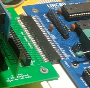
The LiNC 5-slot Z50Bus backplane is to be counted as a reference implementation of a Z50Bus expansion backplane. The SC128 – Modular Backplane for Z50Bus by Stephen C Cousins is the alternate reference.
Limitations
The z50Bus definition has few lines reserved for interrupt handling outside IM2, and few lines for DMA and Bus Mastering. The bus is intended to provide core functionality common across Z80-based systems, with some flexibility to support other 8-bit processors. Systems that want/need to implement nested interrupts with several lines, need complex (full featured) bus mastering, or system specific lines not present on the Z50Bus need to implement these features using either a secondary system specific bus connector, or flying leads.
The pin-out used for host connectors as demonstrated by the LiNC80 SBC1 connects the system board IEO to the IEI pin of the first card connected to a system bus backplane, such as the LiNC 5-slot Z50Bus backplane. This leads to a limitation where an IM2 interrupt enabled expansion card is supported only when plugged into a backplane. Plugging such a card directly to the Z50Bus expansion connector of a host system will leave the card’s IEI line disconnected, and the system IEO output connected to the expansion card’s IEO output (creative users may find a suitable workaround, but this is not officially part of the standard).
I/O address recommendations
LiNC does not set hard requirements or restrictions on I/O address space for the Z50Bus. The Z50Bus as described here is indended to be a bus specification. This means it should define signals, connector and physical requirements, but should be careful about defining system requirements or address space allocation unless it is required to make the bus work. Definition of I/O address requirements is a task for the system integrator, i.e. the one who chooses to implement the bus on system- and expansion boards.
However, to retain broad compatibility between devices from different implementers, a general suggestion for the use of the relatively limited I/O address space has been outlined in collaboration with the first integrators outside of LiNC.
| I/O Address | Use (General) |
| 0x00 to 0x3F | Processor card or SBC or Motherboard, and cards operating specifically with these devices. |
| 0x40 to 0x4F | Available to third party vendors. |
| 0x50 to 0x5F | Available to third party designs/vendors. Alternative addresses for some LiNC cards. |
| 0x60 to 0x7F | Specialist cards where address clashes are not likely. |
| 0x80 to 0xAF | Core cards with well specified functions. Vendors encouraged to map compatible cards here. |
| 0xB0 to 0xBF | Available to third party vendors. |
| 0xC0 to 0xDF | Available to third party vendors. |
| 0xE0 to 0xFF | User’s own designs (suggested addresses). Do not use for products that are to be sold. |
Stephen C Cousins has put together a spreadsheet with most known devices (as of Jan 2019) of both RC2014 and Z50Bus. Mr. Cousins was the first implementer of the Z50Bus after LiNC published the specification, and was also central in the discussion about the general recommendations on address space use. Documentation about Mr. Cousins implementation is located on his page about the Z50Bus, located at https://smallcomputercentral.wordpress.com/z50bus-4/
Using the Z50Bus with the 6502
Being a bus for 8-bit microcomputers designed after 2016, the number of potential CPU’s relevant for new designs is limited. Currently only the Z80-family and the 65×02 family of CPU’s have parts still in production. Because of this, only a 65×02 adaption of the bus is suggested here.
Some of the Z80-style signals need to be synthesized. 65×02 uses memory mapped IO, so the IOReq signal needs to be generated by the CPU card/system when a request is made to the 65×02 IO address space selected for the system. The Mreq signal will then be a simple invert of the IOReq signal. An equivalent function of the WAIT and HALT signals may be found on the 65×02 RDY line. A diode split of the function may be appropriate. The SYNC signal can be adapted for the M1 signal function, if the INTAck feature is considered in the implementation.
| 65C02S signal | Z50Bus | Z80 signal | RC2014 |
| *SYNC | M1 | M1 | N/A |
| (generated) | MREQ | MREQ | MREQ |
| (generated) | IOREQ | IOREQ | IOREQ |
| *R/W | RD | RD | RD |
| R/W | WR | WR | WR |
| N/A | RFSH | RFSH | N/A |
| (RDY) | HALT | HALT | N/A |
| (RDY) | WAIT | WAIT | N/A |
| INT | INT | INT | INT |
| NMI | NMI | NMI | NMI |
| RES | RST | RESET | RST |
| BE (Jump) | BUSRQ | BUSRQ | N/A |
| N/A | BUSAK | BUSAK | N/A |
| PH2 (clk out) | CLK | CLK | CLK |
| A0-A15* | A0-A15 | A0-A15 | A0-A15 |
| D0-D7 | D0-D7 | D0-D7 | D0-D7 |
| ML (Jump) | USR0 | ||
| VP (Jump to GND) | |||
| SO | USR1 |
There exists a 65c02 CPU card for the RC2014 system, this should be seen as the reference implementation when adapted to Z50Bus layout for the basic signals. See http://ancientcomputing.blogspot.no/2017/05/a-6502-cpu-for-rc2014-part-1.html. It is suggested that 65×02 based systems using the Z50Bus indicate clearly that not all expansion cards designed for a Z80 native Z50Bus system will be compatible.
Support products
The products listed under this heading are the products made available by LiNC to support development of Z50Bus based systems.
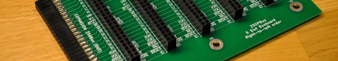
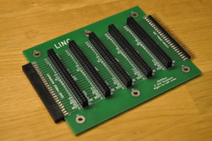
5-slot backplane
A 5-slot back-plane with pass-through connections is available. The back-plane is designed to accept five expansion cards, and to connect to a host system using a male Z50Bus connection on the right side. The pass-through connector is placed on the left side, allowing for daisy-chaining of multiple back-plane cards. This card is fully passive, so any buffering needs to be done on either the host system, or on the expansion cards.
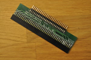
Z50Bus to RC2014 adapter
This simple adapter allows connection of RC2014-compatible expansion cards on a Z50Bus, or fast prototyping of native Z50 cards by using single-row header connectors during initial prototyping stages
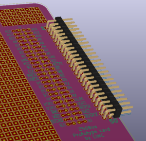
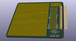
Z50Bus Prototype Card
This is a perf-board style prototyping card, with a full Z50Bus connection conveniently brought out on easily available pads.
Products using Z50Bus
LiNC does not expect to be able to track all Z50Bus devices. Without including the above mentioned productrs, this list includes devices where LiNC has been involved, either designing, providing information about the implementation, or verified the implementation.
- LiNC80 SBC1 by LiNC. The first system to implement the Z50Bus. Features all the “core” Zilog Z80 family parts: CPU, SIO/2, CTC and PIO, providing async serial (and possibility for sync serial), parallel I/O ports and timers, and is designed to be expanded using the Z50Bus.
- Z50Bus Simple digital I/O card by LiNC
- Z50Bus AY3-8910/YM2149 Sound card by LiNC
- SC501 – 7-slot Backplane by Stephen C Cousins.
- SC502 – Power and Reset Card by Stephen C Cousins.
- SC503 – Z180 Processor Card by Stephen C Cousins.
- SC504 – Compact Flash Interface Card by Stephen C Cousins.
- SC505 – Real Time Clock Card by Stephen C Cousins.
- SC506 – Digital I/O Card by Stephen C Cousins.
- SC507 – 3-slot Backplane by Stephen C Cousins.
- SC508 – 10-slot Backplane by Stephen C Cousins.
- SC509 – Z80 PIO (Parallel I/O) Card by Stephen C Cousins.
- SC510 – Prototyping Card by Stephen C Cousins.
- SC118 Z80 Processor Card for Z50Bus by Stephen C Cousins. This card uses the Z50Bus as a central CPU/System bus, and thus uses a pin-out intended to plug as a “card” on the bus, rather than using it as an expansion bus where the CPU/SBC card plugs into the “host” side of the bus.
- SC140 Z180 Processor Card for Z50Bus by Stephen C Cousins. This card uses a Z180 CPU, the “big brother” of the Z80. On the software side, it is desgined to run RomWBW, and can also be used with SCM. The card can be used as a stand alone SBC, or as the central part of a Z50Bus system. It includes async serial and SPI on-board. Like the SC118, the SC140 connects to the Z50Bus as a “card”.
- SC125 – Serial Card for Z50Bus by Stephen C Cousins
- SC127 – Compact Flash Card for Z50Bus by Stephen C Cousins
- SC128 – Modular Backplane for Z50Bus by Stephen C Cousins. Compatible with both hosts using the bus as a system expansion and with cards using the bus as a CPU bus (e.g. SC118).
- SC109 – Modular Backplane for Z50Bus & RC2014+ by Stephen C Cousins. Same compatibility as SC128, plus compatibility with RC2014 on both 40-pin bus, expanded bus and 80-pin bus.
- SC117 Prototyping Breakout Board for Z50Bus by Stephen C Cousins
- SC144 RTC & I2C Card for Z50Bus by Stephen C Cousins