

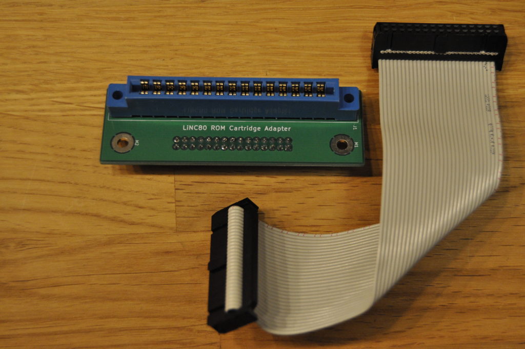
The LiNC80 SBC1 has an on-board connector designed to connect to a card-edge connector for rapid and accessible swapping of ROM. This is the kit that enables the use of the ROM Slot connector, letting you swap ROM content quickly and easily by using ROM Cartridges. The kit consists of ROM Card, optionally a ZIF socket or DIL socket, an adapter PCB with mounting holes, a 30-pin 805-series card edge connector, one 2×15 pin 2.54mm pin header, two 30-pin female IDC connectors, and a 30-wide ribbon cable.
The IDC-to-cardedge adapter PCB is a purely passive adapter, with a pin-for-pin connection for all 30 pins. This means it can be used as a general pinheader/IDC-to-cardedge adapter in addition to its intended use.
The ROM Card/cartridge is designed to be large enough to comfortably insert and remove. It has a 28pin location for either a direct soldered or socketed ROM chip, and a central mounting hole for encased cartridges. The two two-position jumper locations allow for any ROM chip size between 16 and 64kByte, taking advantage of the LiNC80 ROM Bank select signals for ROM sizes above 16kByte. If your ROM application fits in a 4k or 8k chip, it’s naturally no problem to use chips of those sizes, as the pinout on the connector is JEDEC compliant.
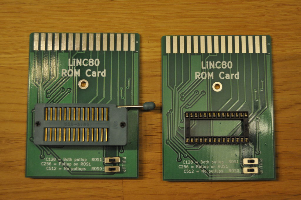
As noted on the silk-screen: select (or solder-bridge) jumper positions according to the size of ROM chip installed on the card. When installing a 4k, 8k or 16k ROM chip (C128 and smaller), both jumpers must be set to PULLUP for proper operation. If using a 32k ROM chip (C256), the ROS1 jumper needs to be set to PULLUP to correctly connect the Vpp pin to VCC. For a 64kByte C512 chip, it is recommended to use the ROSx-position on both jumpers. For more information about the ROS-signals, refer to the configuration register documentation in the LiNC80 SBC1 onboard devices guide. Note that the PCB-mounted switches shown in the picture aboveare not included.
To use this cartridge PCB with your own design, please refer to the LiNC80 SBC1 ROM Slot documentation for information about the pinout. Pin numbering on the card-edge is odd-even, as presented for the 30-pin header connector, with odd-numbered pins on the top silkscreened side.
Ordering options include:
- Full kit, includes ROM Card PCB, Adapter PCB, a 30-pin 805-series card edge connector, one 2×15 pin 2.54mm pin header, two 30-pin female IDC connectors, and a 30-wide ribbon cable
- Full kit with ZIF socket, includes the parts in the Full Kit, plus a 28 pin Zero Insertion Force socket
- Full kit with DIP socket, same as above, but with a conventional stamped-pin DIP socket instead of a ZIF socket
- ROM Card only, includes only a ROM Card PCB
- ROM Card with ZIF socket, includes a ROM Card PCB and a ZIF socket
- ROM Card PCB and adapter PCB, boards only (no connectors, sockets or other components)
The Full kit versions include a printed copy of the assembly guide.
The ROM Cartridge Slot is provided in kit-form only, assembly and soldering is required.