
- Two serial ports
- Counter/Timer circuit
- Configuration register
- Two parallel ports
- 8-bit IDE for Compact Flash
- I/O address map details
The serial ports
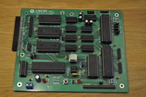
With the first generations of microcomputers, the serial port was the way to talk interactively to the system. LiNC80 SBC1 is no different, as it has no graphics capabilities in its standard configuration. Using the serial port to connect a terminal, either in the form of a modern PC with a software terminal, or connecting a hardware terminal, is the way you will interact with the system. The LiNC80 SBC1 provides not one, but two separate serial ports, and you choose at boot what port you want to use as your console. The other port is then available for other uses if you wish!
The serial ports are implemented using the Zilog Z80 SIO/2, connected to be used as a Dual UART. The SIO/2 chip actually a dual-channel multi-function peripheral component designed to satisfy a wide variety of serial data communications requirements in microcomputer systems, synchronous, asynchronous, serial-to-parallel, including support for high-level protocols such as BiSync, HDLC and SDLC. Because the LiNC80 SBC1 only connects the signals needed for standard asynchronous serial communications, most of these features are unavailable.
The two ports of the serial controller, SIOA and SIOB have been given different electrical interfaces. The first serial port, SIOA is connected to a MAX232 compatible RS232 line driver/transceiver. The board connector for this port uses the DTK/Intel pin layout, making it easy to convert this to a standard DB9 or DB25, without wasting the space (or cost) of a board-soldered DSub connector.
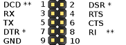
Factory made IDC10DTK-DB9 cables are available from several sources, like this one from logic supply. Of the 10 pins, four should be given special mention. Pin 2 and 7 (*) are directly bridged on the PCB, and not connected to the SIOA . This makes the DTE you connect see “itself” on the DTR/DSR signals. Pins 1 and 8 (**), DCD and RI are not connected. This has been done to simplify the design and construction, as it is not expected that the on-board serial port will be used to drive a traditional analogue modem.

SIOB is provided as a bare TTL compatible 5V serial port. The pin-out of this connector has been chosen to be compatible with the pseudo-standard of the “FTDI Cables” that became very popular with the first generations of Arduino. This port is ideal for connecting a USB-to-5V-serial adapter. SIOB is also connected to the TX and RX lines of the Z50Bus

I/O address range for the SIO/2 is 0x00 to 0x03. The two first addresses are data port A and B, the final two are control register A and B, respectively. These addresses have simple decoding, so all four addresses are echoed at 0x04-0x07.
Serial communication speed of the two serial ports are defined by their software configuration, and their jumper settings. CLK select jumpers J2 and J3 are used to select between system/CPU clock and CTC outputs as source for the async transceiver clocks. Placing the jumper on positions 1-2 selects CTC ZC output, while jumping pins 2-3 selects CPU clock.
The default setting for the CLK jumpers when using ROM image 1.0 is
- J2 SIOA to CTC source (1-2)
- J3 SIOB to CPU source (2-3).
The defaults in software selects 9600bps for SIOA, clocked by channel 0 of the CTS, and 115200bps for SIOB, clocked by the system clock. Both ports are configured for 8 bit data, no parity, 1 bit stop (8-n-1).
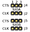
CTC select jumpers J4 and J5 selects the connections of the SIOA and SIOB CTS inputs respectively. Position 1-2 connects the CTS input to the serial connectors, activating the CTS signal input. Position 2-3 ties the input to ground, effectively disabling the use of the CTS input signal. The SIO CTS inputs are active low, so tying it to ground makes the SIO think it’s always clear to send.
The Counter/Timer
The Z80 CTC is available at I/O address range 0x08-0x0B. This device is a four-channel counter/timer that can be programmed by system software for a broad range of counting and timing applications. These four independently programmable channels satisfy common microcomputer system requirements for event counting, interrupt and interval timing, and general clock rate generation.
The CTC allows easy programming: each channel is programmed with two bytes; a third is necessary when interrupts are enabled. When started, the CTC counts down, automatically reloads its lime constant, and resumes counting. Software timing loops are eliminated.
Counter/Timer operation can be run either as a timer driven by the common clock input signal, or as a counter driven by separate Clock/Trig inputs per channel. Three of the channels have a Zero Crossing/Timer Output, a logic level signal that goes Active when the Counter/Timer crosses zero. All four channels may generate interrupts. Interrupt processing is simplified because only one vector needs to be specified; the CTC internally generates a unique vector for each channel.
On the LiNC80 SBC1, the four channels have been assigned separate, but flexible tasks. Channels 0 and 1 are wired with their Zero Crossing/Timer Output signals to the two serial port clock signal selectors, while the system clock is used as as clock/trig inputs. This allows for flexible serial transceiver rate clock, by using the CTC programmable channels to select the serial rate. When the serial port transceiver clocks are set to use the System clock, the CTC channel becomes available as a general timer/counter for interrupt driven tasks.
Channel 2 also runs of the system clock. It’s output is connected to the clock/trig selector jumper of Channel 3. This allows Channel 3 to be driven by either the SYNC signal from an external device, or as a cascaded counter/timer, cooperating with Channel 2.
The TRG3 SEL jumper J7 allows for selection of the input clock/trigger signal for CTC channel 3. Jumping positions 1-2 selects the ZC/TO output of channel 2 as CLK/TRG input of channel 3. Selecting position 2-3 wil connect the MEMBANK connector’s SYNC signal as CLK/TRG3. Pin one of J7 is the pin closest to the J7 label on the PCB.
Configuration register
To provide the functionality of being able to map ROM out of (and back in) memory, and provide the mechanism for bank-switching of both RAM and ROM, the configuration register at address 0x38 is used. This register is a simple 8-bit write-only data latch, with function-dependent bits. During RESET (and boot) all bits in the register are set to zero.
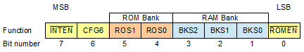
/ROMEN
The least significant bit, bit 0, is the active low /ROMEN bit. Setting this bit to zero enables ROM (and disables the lower 16kBytes of RAM). Setting this bit to one disables ROM, mapping in the lower 16kBytes of RAM in it’s place. Note that this applies to both on-board ROM, and the ROM cartridge slot. This bit is actively used by the CP/M loader, to make the lower part of memory available to CP/M.
BKS[2-0]
The three next bits, bits 3, 2 and 1 make up the 3-bit RAM Bank Select, where the least significant bit is BKS0 on register bit 1. The on-board RAM occupies RAM Bank 0, bit pattern 000, making that the bank selected at boot and hardware reset.
ROS[1-0]
Bits 5 and 4 are the ROM Bank Select bits, where bit 5 is ROS1 and bit 4 is ROS0. The ROM BANK Select bits are available on both the MEMBANK connector and the ROM Slot connector, providing flexibility in expansion. Note that if a ROM add-on card is used on the Z50Bus in combination with MEMBANK, the OB_ROM jumper J6 should be set to the “OFF” position (pins 2-3).
On the LiNC80 SBC1, there are two ROM configuration jumpers, J8 and J9. Those were originally added to make support of different size ROM chips possible, but by using a 64kByte ROM chip, and setting both of the jumpers in the SELECT position, the ROM Select bits will select between the four possible blocks of ROM.
CFG6
This bit is an extra configuration bit, present on the memory bank connector, but has no current defined function. System integrators are recommended to treat this bit as a reserved bit with undefined function. Until this documentation changes, the value of CFG6 should be zero.
/INTEN
The avtive low /INTEN bit located as MSB (bit 7) of the configuration register controls the Interrupt Enable In of the first I/O device of the system. This functions as a Master Interrupt Enable in hardware. But setting this bit to one, no hardware devices that honor the IM2 interrupt system can generate an interrupt, as they see the high input of the IEI as a higher priority device blocking interrupts. Also because this uses the IM2 behaviour, the interrupt priority chain will resolve as normal when the /INTEN bit is set back to zero. So where a CPU DI instruction will disable interrupts and ignore them, using /INTEN makes the interrupt chain block until the bit gets cleared again.
Parallel ports
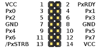
Two parallel, programmable digital I/O ports are available on the Parallel Port A and B connectors. These two ports are provided by a Z80 PIO, located at I/O addresses 0x18 to 0x1B. The two I/O ports (A and B) are virtually identical and can used to interface directly to peripheral devices. By using the PIO control register, the ports can be configured for byte input, byte output, with or without strobe signals, or in bit control mode, where each of the 8 bits can be individually configured as input or output. Interrupt generation is available in both byte and bit-control modes. Note that the PIO uses the RDY and /STB signals for gating and latching handshaking when used in byte modes. System integrators that wish to remain compatible with future LiNC80-based microcomputers should note that PIOA may be reserved for internal use on future systems.
8-bit IDE connector
Before the 16Bit AT Attachment (IDE, ATA, PATA), there was a precursor, XT-IDE, that used an 8-bit data path and simpler control logic. One of the communication methods for XT-IDE was a 8-bit memory-oriented mode. Modern Compact Flash cards are to a large degree PATA devices with a compact connector, but they also are required to support this 8-bit legacy communication method.
On the LiNC80 SBC1 this is exploited, by providing a 40-pin connector with an IDE layout, but only configured to use the signals needed for 8-bit mode of CF cards. The choice of a 40-pin connector in place of a direct CF-connector comes from two points: a CF-connector uses a very dense pin spacing, and is only available as a surface mount device, and the the cost of a CF-connector in low quantities can be higher than purchasing a complete IDE-to-CF adapter, where the CF connector is already soldered to a board with a 40-pin connector.
These factors mean that the 8-bit IDE connector is only compatible with Compact Flash, and to connect a Compact Flash card, an IDE-to-CF adapter is needed. We have currently only verified one such adapter, the IDE2CF adapter from StarTech. These are available from StarTech directly, or through Amazon.com. Other passive IDE-to-CF adapters should work just as well. While not yet tested, the SB-ADIDE2CF-B1 adapter from Monoprice looks elegant.
Connecting your IDE-CF adapter is as simple as using a short IDE cable, or direct insertion if your adapter supports it. If your IDE-CF adapter supports power supply via the IDE connector pin 20, add a jumper to P7 (P20VCC) located directly next to the IDE connector. If your adapter requires external power connection, you will have to tap 5V off your incoming powersupply.
The current ROM and CP/M BIOS/BDOS is limited to use 64MB or 128MB of storage on CF. Not all CF cards can be used with the system, and the larger the card, the less likely it is that it will work. It is recommended to use a CF card of less than 2GB size, with 64MB, 128MB, 256MB and 512MB large cards reccomended. For cards larger than 128MB, the remaining space after 128MB is not used.
I/O address map
On-board device address decoding is naive, so there is quite a bit of I/O address “ghosting”. 1/4th of the total I/O address range is reserved, with the following mapping:
0x00 – 0x07 SIO/2
- 0x00 SIOA Data (Echo at 0x04)
- 0x01 SIOB Data (Echo at 0x05)
- 0x02 SIOA Control (Echo at 0x06)
- 0x03 SIOB Control (Echo at 0x07)
0x08 – 0x0F CTC
- 0x08 Channel 0 (Echo at 0x0C)
- 0x09 Channel 1 (Echo at 0x0D)
- 0x0A Channel 2 (Echo at 0x0E)
- 0x0B Channel 3 (Echo at 0x0F)
0x10 – 0x17 8-bit IDE for Compact Flash
- 0x10 CF Chip Select (all 8 addresses echo this)
0x18 – 0x1F PIO
- 0x18 PIO Port A Data (Echo at 0x1C)
- 0x19 PIO Port B Data (Echo at 0x1D)
- 0x1A PIO Port A Control (Echo at 0x1E)
- 0x1B PIO Port B Control (Echo at 0x1F)
0x20 – 0x37 Not used on-board
- These I/O addresses are reserved for use with future official LiNC80 expansions.
0x38 – 0x3F Configuration Register
- 0x38 Write-only configuration register
(all 8 addresses echo this)
This leaves the I/O address space 0x40 to 0xFF available for expansion devices.