
The base configuration of the LiNC80 with no expansion provides 64kByte of RAM and ROM in 16kByte banks on-board. The standard configuration of ROM only contains data in the lowest ROM bank. During boot, the lower 16kByte of RAM is replaced by the ROM, containing the boot monitor, memory load utility and a port of Microsoft BASIC as run on the Nascom computer. This ROM area can be disabled, and loading CP/M will do just that, deactivating the ROM, making the memory map fully RAM.
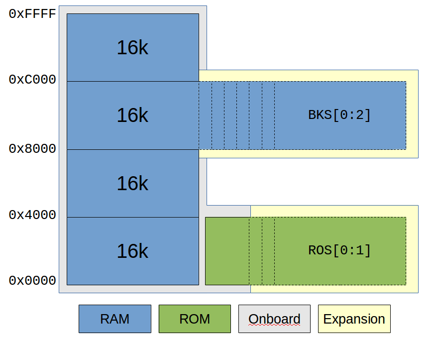
The memory layout of LiNC80 has been designed to use bank-switching to allow expansion. By adding a suitable designed RAM expansion, a 16kByte window of the memory map can be banked across up to 8 separate banks. To select RAM bank, the bits 1-3 (BKS0-2) of the write-only configuration register at I/O address 0x38 are used. RAM bank 0 maps to the on-board memory, all other banks are expected to be added on expansion card, using the MEMBANK connector signals to map out the banks.
In addition to bank-selection of RAM, bank-selection is also available for ROM. Configuration register bits 4-5 (ROS0-1) allows selection from one of four ROM banks. The standard configuration only contains data in bank 0, but by using the ROM Cartridge slot, ROM chips using all four banks can be used.
By setting bit 0 (/CFG_ROMEN) of the configuration register to 1, ROM gets disabled. This allows for a full 64kByte RAM memory. Software running from RAM can map ROM back into memory by setting the /CFG_ROMEN bit back to 0 (this should not be done when running CP/M).
Because LiNC80 allows for up to 7 extra RAM pages, the maximum RAM configuration can be 176kBytes. With 4 ROM pages available for use, either on-board or on expansion, up to 64kBytes of ROM can be equipped. This allows for a significantly expanded system. This memory layout is not designed for big-memory systems like RomWBW or Fusix, and will not run them without major modifications.
Detailed memory information
0x0000 – 0x3FFF ROM/Lower 16K
During boot, the lower 16k is banked to the first ROM block (bank 0). The standard ROM map contains:
- ROM Bank page 0: Small Computer Monitor, Microsoft/Nascom BASIC, CPM loader
- ROM Bank page 1: Grant Searle’s Monitor/Loader, Microsoft/Nascom BASIC
By setting the /CFG_ROMEN bit of the configuration register (bit 0 of IO addr 0x38) the ROM gets disabled, and replaced by RAM. This is done when using the CP/M loaders, and when CP/M is loaded, the lower memory contains:
- 0x0000 RST00 vector – CP/M Boot, 2 bytes
- 0x0003 IOBYTE, 1 byte
- 0x0004 Current Drive, 1 byte
- 0x0005 BDOS entry vector, 3 bytes
- 0x005C Default FCB and RR, 36 bytes
- 0x0080 TPA Buffer, 128 bytes
- 0x0100 -> Transient Program Area
0x4000 – 0x7FFF
This part of memory always points to on-board RAM (upper half of the lower 32k RAM chip).
0x8000 – 0xBFFF
Bankable RAM area. On boot, on-board RAM (bank 0) is selected. If the system has been expanded with additional memory banks, selected through configuration register bits 1-3 (BKS0-2), this window is where the bank-switching is done. Note that RAM banks 6 and 7 (0b110 and 0b111) are reserved for graphics expansion.
0xC000 – 0xFFFF
Top of memory. This section always maps to on-board RAM (upper 16k of the high 32k RAM chip). If CP/M is used, it contains:
- 0xD000 CCP
- 0xE600 BIOS
ROM related jumpers
There are three jumpers on-board that determine ROM behavior. The jumper J6 enables or disables the on-board ROM completely by disabling its chip-select signal. This feature allows for expansion cards that replace the on-board ROM functionality. In normal operation, this jumper should be set to position 1-2 (ON).
The two jumpers J8 and J9 allows override of the ROS0 and ROS1 signals. The middle pins are connected to the ROM socket, their pin 1 are connected to VCC, and their pin 3 to the ROM-select signals ROS0 and ROS1. The standard kit ships with a 32kByte ROM, and the pin connected to J9 needs to be tied to VCC, easily accomplished by strapping J9 on pins 1-2.
With the default ROM and using default jumper positions (J8 = Select 2-3, J9 = High 1-2), the system will boot to SCMonitor from ROM Bank page 0. If J8 is moved to High 1-2, you’ve effectively overridden the ROS0 signal and selected ROM Bank page 1, and your system will boot to the Grant Searle monitor/loader.
The jumpers allow for a very varied selection of ROM chips, types and configurations. Rather than describing in detailed length each combinations, we chose to refer to these two excellent documents provided by S.C.Cousins:
- ROM-Pin-mapping.pdf (Shows the relationship between the ROM socket and ROS-signals with common ROM chip types. Pins that have multiple functions are highlighted in bold text)
- SCMon-v1-0-installation-e1-0-0.pdf (Describes how to set jumpers for SCMon using various ROM types, and how to build your own SCMon ROM)
ROM cartridge connector
To make ROM software flexible, a connector for ROM expansion is provided, inspired by the ROM Cartridges popular on 8-bit home computers.
To make use of this connection easy and true its the retro-computing nature, a set of cable, PCB and connector for use with card-edge connectors is available in our LiNC80 ROM Cartdrige Slot kit.
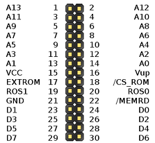
The ROM expansion connector maps out only memory-related signals from the CPU, but includes the ROM Select signals from the configuration register. The EXTROM signal on the connector should be connected to VCC by any ROM cartridge, as doing that disables the on-board ROM, letting the cartridge replace it. By using our ROM Cartridge PCB or Kit, this is already implemented.
Memory expansion connector
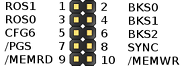 To allow design of memory expansion without making changes to the existing Z50Bus expansion, a separate 10-pin connector contains the signals needed to provide both RAM and ROM banking. On this connector, the CPU signals /RD, /WR and /MReq are combined into two convenient signals, /MEMRD and /MEMWR. The SYNC signal is provided to allow trigger-pulses to be sent to the Counter/Timer circuit, and can e.g. be used for video sync signal counting.